STM32F103 vs GD32F103: The Pin-Compatible Alternative
STM32F103 vs GD32F103: compare the pin-compatible MCU alternatives by core, clock, register map, peripherals, and the firmware porting the swap needs.
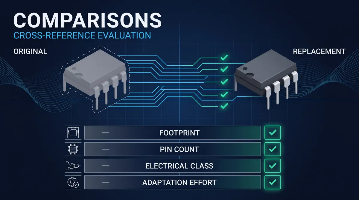
STM32F103 vs GD32F103 is the defining comparison of the domestic alternative market, because the GD32F103 is the best-known attempt to reproduce the STM32F103, one of the most widely used microcontrollers of the last generation, on the same pins and largely on the same software. The STM32F103 is STMicroelectronics' classic Cortex-M3 microcontroller, the part that powered a generation of boards from industrial controls to the famous Blue Pill, and the GD32F103 is GigaDevice's pin-compatible alternative, a Cortex-M3 part built to fit the same LQFP48 footprint and to run much of the same firmware. The comparison matters because the STM32F103 has been scarce, priced up, and supply-constrained, and the GD32F103 is the practical answer for a buyer or an engineer who wants the board to survive without a redesign. This guide compares the two across the package, the core, the clock, the memory map, the registers, the peripherals, and the firmware migration, and it is deliberately honest about the compatibility: the GD32F103 is pin-compatible and largely software-compatible, with documented differences that a bring-up test surfaces, and the guide says where the differences live.
The comparison is also the working example of the pin-and-code-compatible replacement that this site's catalog is built around, and it is the case that teaches the whole category. A board that used the STM32F103 does not have to be redesigned to use the GD32F103, because the LQFP48 footprint matches, and the firmware does not have to be rewritten from scratch, because the core and much of the register map match, but the swap is not a thoughtless drop-in either: the clock configuration, the peripheral initialization, and some peripheral behaviors differ, and the differences are exactly what a structured porting and bring-up qualifies. This guide gives that structure, and it is the honest, engineering-first comparison that a designer needs before committing a production line to the alternative.
STM32F103 vs GD32F103: The Compatibility Claim
The GD32F103 against the STM32F103 is a claim about two levels of compatibility, and reading the claim precisely is the first step of the comparison. The pin compatibility is the physical level: the GD32F103 is offered in the same LQFP48 package and places the same functions on the same pins as the STM32F103's LQFP48 package, so the board that mounts the STM32 mounts the GD32 without a re-layout, and the power, the ground, the oscillator, the reset, the boot, and the GPIO and peripheral pins match. The software compatibility is the second level, and it is the qualified claim: the GD32F103 uses the Cortex-M3 core and a register map designed to be largely compatible with the STM32F103, so much of the firmware compiles and runs after the migration, but the compatibility is not total, and the differences live in the clock tree, some peripheral registers, the ADC, and other details that the migration note and the bring-up test reveal. The honest summary is that the GD32F103 is pin-compatible and largely register-and-software-compatible, and the guide reads the claim at that level rather than as a promise of a perfect drop-in.
The two parts also match on the headline package and capacity, which is the fact that makes the comparison practical. The STM32F103C8T6 and the GD32F103C8T6 square off directly: both are Cortex-M3, both are LQFP48, both carry the 64-kilobyte flash and the 20-kilobyte SRAM of the C8 grade, and both run the classic 72-megahertz-class clock that the family is known for, with the GD32 part offering headroom beyond it in some grades. The matching headline tells the buyer that the GD32F103 is built to occupy exactly the STM32F103's place, and the differences are in the implementation rather than in the shape, which is why the comparison is a migration story rather than a redesign story. The compatibility claim is the frame of the whole comparison, and the rest of this guide reads the claim against the package, the core, the registers, and the behavior.
What compatibility the GD32F103 actually delivers
The GD32F103 delivers pin compatibility as a guarantee and software compatibility as a documented, mostly-true claim, and the distinction is the fair statement of the market. A designer who needs the LQFP48 footprint and the pin functions can mount the GD32F103 and trust the pins, because the pinout is designed to match and the datasheet states it. A designer who needs the firmware to run as-is is in a different position: the GD32F103 runs the Cortex-M3 instruction set and a largely-compatible register map, so the firmware compiles for the GD32 with its own CMSIS and its own startup, and the clock and the peripheral initialization are where the differences appear. The compatibility the GD32 actually delivers is therefore the combination, the pins as a guarantee, the software as a compatible-and-checked claim, and the professional uses of the part read the migration note, adapt the firmware, and run the bring-up rather than assuming the binary from the STM32 runs unchanged.
Package, Pinout, and Footprint: STM32F103 vs GD32F103
The package and the pinout are the first and the most solid layer of the comparison, and the GD32F103 matches the STM32F103 where the board lives. Both parts ship in the LQFP48 package, the same 48-pin, 7-by-7-millimeter low-profile quad flat pack with the same pin pitch and the same pad geometry, so a board laid out for the STM32F103's LQFP48 footprint accepts the GD32F103's LQFP48 body without a change. The pin functions match across the supply, the ground, the VDDA and the VSSA, the oscillator and the reset, the boot pins, the SWD debug pins, and the GPIO and the peripheral alternate functions, and the lead assignments are designed to line up. The footprint is the contract of the swap, and it is the strongest reason the GD32F103 is a replacement rather than a redesign, because the board, the assembly, the test fixture, and the pick-and-place program all survive the change.
The pinout also reads the alternate functions with care, because the microcontroller pins carry many functions through the multiplexer, and the alternate function map is where a pin-compatible claim can hide a difference. The GPIO ports and the USART, the SPI, the I2C, the timer channels, and the ADC channels that the firmware assigns through the alternate function registers must live on the same pins on the GD32F103 as on the STM32F103, and the migration note and the datasheet tables state the mapping. The designer who ports the firmware verifies the alternate function placement the firmware uses, rather than assuming that a shared pin name means a shared function on every multiplex, and the verification is part of the porting checklist. The package and the pinout are the physical anchor of the comparison, and the alternate function check is the fine print that keeps the anchor true.
The LQFP48 footprint and pin mapping compared
Comparing the LQFP48 footprints side by side places the two parts on the same board. Both are 48-pin quad flat packs with a 7-millimeter body and the 0.5-millimeter pin pitch, and the pin 1 orientation and the pad layout are the same, so the reflow and the inspection follow the same recipe. The pin mapping walks the same order, the power and the ground on their fixed positions, the oscillator pins, the NRST reset, the BOOT0 pin, the SWD pins, and the GPIO organized by port with the alternate functions assigned by the same multiplexer scheme. A board that placed the STM32F103 and a board that places the GD32F103 use the same footprint symbol, and the comparison's physical half is a match. The LQFP48 mapping is the reason the swap preserves the board, and it is the half of the comparison that needs no qualification, which is the honest statement the datasheet makes.
Core, Clock, and Performance: STM32F103 vs GD32F103
The core and the performance are where the two parts match at heart and differ in the implementation. Both use the ARM Cortex-M3 core, the same 32-bit architecture with the same Thumb-2 instruction set and the same debug and interrupt infrastructure, so the compiled firmware's instruction-level behavior is the same and the toolchain and the debugger are the same. The clock is where the implementation differs: the STM32F103 runs at a maximum of 72 megahertz, and the GD32F103 is built to run at the same 72-megahertz class with headroom in the part's design, and the clock tree that generates the system clock from the oscillator through the PLL has the GD32's own configuration, so the firmware's clock initialization code has to be adapted to the GD32's PLL registers rather than copied unchanged. The performance comparison is therefore the same core at a compatible clock, with the clock configuration as the first porting task, which is the honest engineering read of the two parts.
The compiler and the toolchain deserve their own note, because the migration runs through them. Both parts are supported by the ARM toolchain and the mainstream IDEs, and the GD32F103 brings its own CMSIS device header, its own startup file, its own system-clock file, and its own standard peripheral library, which the engineer adds to the project instead of the ST's firmware library. The firmware that was written against the ST's peripheral library or the ST's low-level drivers has to be adapted to the GD32's library, and the firmware that was written at the register level has to be checked register by register, which is where the compatibility claim becomes work. The porting is the real cost of the swap, and it is the reason the comparison treats the GD32F103 as a largely-compatible part with a migration, not as an identical drop-in. The core is the match, the clock is the difference, and the migration is the work between.
How the clock configuration differs between the two
The clock configuration is the first and the most concrete porting task, because the STM32F103 and the GD32F103 generate their system clocks through similar but not identical PLL schemes. The firmware that configures the ST's clock, the oscillator, the PLL, the system clock switch, and the bus prescalers, has to be ported to the GD32's clock-control registers, whose bit layout and reset values differ in the details, and the port sets the system clock the way the GD32's datasheet and the migration note describe. The configuration also sets the peripheral clocks, the APB1 and the APB2, whose prescalers feed the timers, the USARTs, the SPI, and the ADC, and a mistake in the clock port shows up as the wrong baud rates, the wrong timer periods, and the wrong ADC sampling, which is why the clock verification is the first thing the bring-up checks. The clock port is work, but it is bounded work, because the architecture is the same Cortex-M3 and the clock tree is the same shape, and the migration note states the differences. The clock is where the GD32F103 stops being an identical drop-in and starts being a qualified alternative, and the port is the first page of the qualification.
Memory Map and Register Compatibility: STM32F103 vs GD32F103
The memory map and the register compatibility are the software layer of the comparison, and they decide how much of the firmware ports. The memory map is largely compatible: the flash and the SRAM sit in the same address regions, the peripheral registers sit at the same base addresses for the major blocks, and the Cortex-M3's system and debug region is standard, so the linker script and the memory layout carry over with the device definitions. The register compatibility is the qualified claim: the major peripherals, the GPIO, the timers, the USART, the SPI, and the I2C, have registers at the same addresses with largely the same fields, and the differences live in the fine detail, some control bits, some status bits, some reset values, and some peripheral-specific registers that the GD32 implements its own way. The professional read is that the register map is largely compatible at the level the standard drivers use, and the firmware written at the driver level ports with the library adaptation, while the firmware written at the raw-register level demands the register-by-register check.
The register map also reads the areas where the two parts genuinely differ, and the differences are the ones the migration and the bring-up focus on. The ADC configuration, the USART baud-rate calculation, the USB peripheral implementation, and some timer behaviors are known areas where the GD32F103's implementation differs from the STM32F103's, and a firmware that drives those peripherals expects the ST's exact behavior has to be adapted and tested rather than assumed compatible. The migration note and the GD32's peripheral library document the differences, and the engineer reads them for the peripherals the firmware actually uses before the bring-up runs. The memory map is the compatible foundation, the register map is the largely-compatible middle, and the peripheral differences are the specific work, and the three are why the GD32F103 is a solid alternative with a documented port rather than a silent drop-in.
Peripheral differences between the STM32 and the GD32
The peripheral differences are the honest detail of the comparison, and naming them is the discipline that keeps a migration from assuming compatibility. The ADC is a known area, because the GD32F103's ADC configuration, its channel mapping, and its sampling behavior differ in ways that the firmware's initialization and the reading loop have to adapt to and then verify against the actual converter output. The USART is another, because the baud-rate register and some control bits differ, so the serial initialization ports to the GD32's library and the actual baud rate is verified on the wire. The USB peripheral is a third area that the community reports needing attention, because the GD32F103's USB implementation differs from the ST's and a USB stack written for the ST's peripheral requires adaptation. The timer set is a fourth area of detail, because some timer features and behaviors differ in the GD32's implementation. None of the differences is a wall, but each is a task, and the engineer who ports a firmware that uses the ADC, the USART, the USB, or the timers plans the task and verifies the result in the bring-up rather than assuming the port is free.
Firmware Porting and Bring-Up: STM32F103 vs GD32F103
Porting the firmware from the STM32F103 to the GD32F103 is a structured migration, and the bring-up test is the gate that qualifies it. The port runs in stages: add the GD32's device files and the library to the project, port the clock configuration to the GD32's clock registers, adapt the peripheral initialization to the GD32's library or to the verified register fields, and rebuild the firmware for the GD32's device definition. The bring-up then runs the same stages on the hardware: confirm the toolchain builds and the target programs, confirm the boot and the clock by measuring the system clock and the peripheral clocks, exercise each peripheral the firmware uses, the GPIO, the USART, the SPI, the timers, the ADC, and the USB, and compare the behavior and the timing with the original STM32F103 on the same board. The bring-up is the referee of the whole swap, because it confirms the pin compatibility on the mounted part and the software compatibility in the running code, and it is the step that turns the migration from a claim into a qualification.
The bring-up also produces the record that the swap needs, because a production change is judged on evidence. Record the clock measurements, the peripheral bring-up results, the serial traffic, the ADC values, the timer waveforms, and the USB enumeration, beside the STM32F103's readings, and record the differences and the adaptations the port required. The record is the artifact that a change-control process accepts and that the next reviewer uses, and it is the reason a GD32F103 swap can be a documented, qualified alternative rather than a bench experiment. The bring-up also sets the porting timeline honestly: a firmware that uses the GPIO, the serial ports, and the timers ports in days, and a firmware that drives the ADC, the USB, and the exotic timer features takes longer, and the estimate comes from the peripheral map the earlier section described. The port is bounded work, and the bring-up is the proof of the boundary, and the two together are the method that qualifies the alternative.
How to run the migration from the STM32 to the GD32
Running the migration from the STM32F103 to the GD32F103 is a checklist that any engineer follows in the same order. Capture the original project and the firmware, and read which peripherals and which driver layers it uses, because the migration scope is set by the peripheral map rather than by the part number. Add the GD32's CMSIS, the startup, the system clock, and the peripheral library for the GD32F103, and build the project against the GD32's device definition, fixing the compiler and the linker errors the device change surfaces. Port the clock configuration, the oscillator, the PLL, and the bus prescalers, to the GD32's clock registers, and port the peripheral initialization to the GD32's library, checking each field the firmware drives. Flash the GD32 on the board that held the STM32, and run the bring-up stages, the boot and the clock, the peripherals, the system test, and the soak across the temperature range. Record the results beside the STM32's, and the swap is qualified when the GD32 matches the STM32 within the product's tolerance. The checklist is the operating shape of the migration, and it is the same shape whether the firmware is small or large.
When to Choose the STM32F103 or the GD32F103
The choice between the STM32F103 and the GD32F103 is the compatibility-versus-availability decision, and it reduces to a clear rule. Choose the STM32F103 when the firmware must run unmodified on the original device, when the design depends on a peripheral behavior that the GD32 does not reproduce exactly, when the toolchain and the library must be the ST's, or when the certification and the approval were granted against the ST part, and the original device is available and affordable. Choose the GD32F103 when the board needs the LQFP48 swap, when the ST part is scarce or priced up, when the design can spend the porting and the bring-up effort, and when the peripherals the firmware uses are the compatible ones, because the GD32 delivers the same board with a supply that the ST scarcity does not constrain. The rule is the funnel of the comparison: the availability decides the trigger, the peripheral map decides the porting cost, and the bring-up decides the qualification, and the choice is the combination of the three rather than a single headline.
The choice also reads the sourcing and the risk view, because the two parts sit in different supply positions. The STM32F103's scarcity is the reason the GD32F103 exists, and the GD32's supply and the domestic ecosystem are the alternative's strength, while the GD32's documentation, the firmware library, and the community differ from the ST's, and the engineer has to work from the GD32's own materials. A team that values the supply continuity reads the GD32 as the strategic answer, and a team that values the ST's ecosystem reads the STM32 as the safe answer, and the comparison's honest frame keeps both visible. The GD32F103 is not a free upgrade to the STM32F103, it is a qualified alternative that preserves the board and requires the migration, and the choice is the engineering group's decision between the original's ecosystem and the alternative's availability.
A quick decision guide for the STM32 and GD32
| Decision | STM32F103 | GD32F103 |
|---|---|---|
| Package and pinout | LQFP48, the reference footprint | LQFP48, pin-compatible |
| Core | Cortex-M3 | Cortex-M3 |
| Memory (C8 grade) | 64 KB flash, 20 KB SRAM | 64 KB flash, 20 KB SRAM |
| Software compatibility | The reference | Largely compatible, with a documented port |
| Clock | ST's PLL configuration | GD's PLL configuration, requires porting |
| Known differences | The reference | ADC, USART baud, USB, some timer details |
| Availability | Scarce and price-constrained at times | Domestic supply, the alternative's strength |
| Best use | Existing ST ecosystem, unmodified firmware | Board-preserving swap when the ST is scarce |
Worked Porting Walkthrough: A GPIO, Timer, and UART Firmware
A worked porting walkthrough makes the migration concrete, and a firmware that uses the GPIO, a timer for the PWM, and a UART at 115200 baud covers the typical ground. The first step is the toolchain: add the GD32F103's device pack and the firmware library to the project, replace the STM32 startup and the device header with the GD32's, and build, fixing the compiler and the linker errors that the device change surfaces. The second step is the clock: port the system-clock configuration to the GD32's clock-control registers, the oscillator, the PLL, and the bus prescalers, because the GD32's PLL scheme differs in the register layout, and verify the resulting system clock with the oscilloscope on the MCO or the clock pin. The third step is the peripheral initialization: port the GPIO, the timer, and the UART to the GD32's library, and the UART is the instructive case, because the baud-rate register of the GD32 differs from the ST's, so the 115200 configuration is re-derived from the GD32's calculation rather than copied, and the terminal test confirms the actual baud on the wire. The fourth step is the firmware loop: run the existing application and confirm the GPIO toggles, the PWM drives its output, and the UART transmits, and the walkthrough is complete when the application behaves on the GD32 as it did on the STM32.
The walkthrough also reads the differences the peripherals surface, and the timer and the UART are where the port usually spends the effort. The timer's prescaler and period registers, and the PWM channels the firmware drives, are checked against the GD32's register map, because a timer with a different prescaler arrangement produces a different PWM frequency until the configuration is ported. The UART's baud register is the classic difference, and a firmware that copied the ST's value without the port produces a garbled stream that the terminal shows, which is the failure that teaches the port's necessity. The walkthrough records each step, the toolchain change, the clock port, the peripheral port, and the application test, and the record is the evidence the migration file needs. The worked example is the model for the whole migration, and it is the model that the common-failures section then reads against.
Measuring the Clock and the Peripherals During Bring-Up
Measuring the clock and the peripherals during the bring-up is the verification half of the migration, and it runs on the oscilloscope and the terminal. Measure the system clock first, probing the MCO output or the crystal and the PLL configuration, and confirm the GD32 runs at the intended frequency, because the clock port is the first thing the migration touches and the wrong clock propagates to every peripheral. Measure the UART next, connecting the terminal at 115200 and sending the known test pattern, and confirm the characters arrive without the framing errors, because a garbled stream is the baud-register mismatch made visible. Measure the timer and the PWM, probing the output pin and confirming the frequency and the duty against the design, and measure the GPIO toggles, the ADC readings if the firmware uses them, and the interrupt latency where the application depends on it. The measurements are recorded beside the STM32's original readings, and the comparison is the evidence that the GD32 matches the original within the product's tolerance, which is the gate the migration crosses.
The bring-up also runs the soak that the datasheet and the product both demand, because the migration that works at the bench can fail at the margins. Run the application across the product's voltage and temperature range, the low supply where the GD32's clock and the regulators behave differently, the high temperature where the ADC and the timing drift, and the load steps where the firmware's behavior changes, and compare the results against the original's recorded behavior. The soak surfaces the intermittent differences that the bench pass misses, and it is the reason the migration is qualified on the product's range rather than on the bench's happy path. The measurement and the soak together are the bring-up, and they are the half of the migration that turns the ported firmware from a claim into a qualified replacement, which is the discipline the comparison guide has applied throughout.
Common Migration Failures and Their Fixes
The migration from the STM32F103 to the GD32F103 fails in consistent ways, and the fixes are short because the failures are known. If the board does not boot, the usual cause is the startup or the clock, the GD32's startup file not added, the vector table not pointing, or the PLL configuration not ported, and the fix is the toolchain step done completely and the clock measured before the peripherals. If the UART garbles, the cause is the baud register, the ST's value copied into the GD32's register that computes differently, and the fix is the GD32's baud calculation and the terminal test on the wire. If the PWM or the timer runs at the wrong frequency, the cause is the timer's prescaler or the clock tree behind it, and the fix is the ported configuration and the measured output. If the ADC reads the wrong values, the cause is the ADC's configuration or the channel map, and the fix is the ported ADC initialization and the calibration against the known reference. If the USB never enumerates, the cause is the GD32's USB peripheral implementation differing from the ST's, and the fix is the adapter or the rework that the migration note describes, which is the known-hardest area of the swap. Each failure has its signature and its fix, and the fixes are the reason a migration that is planned fails less than one that is guessed.
The fixes also carry the discipline that keeps the migration on the rails, and the discipline is the order of the port. Fix the toolchain before the clock, the clock before the peripherals, and the peripherals before the application, because a wrong clock makes every peripheral wrong and a wrong peripheral makes the application wrong, and the order localizes the failures as they appear. Test each stage before the next, the compile, the boot, the clock, the peripheral, and the application, and record each result, so a failure in the application is traced to the peripheral that was not yet verified. The discipline is the same order the worked walkthrough used, and it is the order that turns the migration from a chain of surprises into a sequence of confirmed stages. The common failures and their fixes complete the migration method, and they are the practical bookend to the porting walkthrough, which is the migration's working face in this guide.
The Boot and the Debug Interface During Migration
The boot and the debug interface are the quiet details of the migration, and they deserve a section because a board that programs and boots wrong stops the port before it starts. The BOOT0 pin and the boot-mode configuration of the GD32F103 are read against the STM32's, because the boot source, the flash, the system memory, or the SRAM, is selected by the boot pins, and a board that held the STM32's boot strapping must hold the GD32's the same way, or the chip boots into the wrong memory and the application never runs. The SWD debug interface is the second detail, because the migration programs the GD32 through the same SWD pins, and the debugger and the device pack must recognize the GD32's ID and its debug registers, which is the toolchain step the worked walkthrough covered. The reset and the power-on timing, the NRST pin and the supply ramp that the datasheet describes, are the third, because a board with a marginal reset or a slow supply ramp can fail to start reliably on the new silicon. The boot and the debug reads are the pre-flight of the migration, and they are the checks that a board-bring-up sequence always runs before the peripherals are trusted.
The reading of the GD32's migration note completes the detail, because the manufacturer's own document states the differences that the port must respect. The migration note lists the register differences, the clock differences, the peripheral differences, and the driver changes, and the engineer reads it for the peripherals the firmware uses, marking the ones that matter to this project, and the marked list is the porting scope that the walkthrough executes. The migration note also states the toolchain and the library setup, the device pack, the startup, and the example projects, and the engineer follows it rather than adapting the STM32's project from scratch, because the vendor's own path is the fastest and the safest. The boot, the debug, and the migration note are the preparation of the swap, and they are the reason a port that starts from the vendor's documents fails less than one that starts from the guess. The preparation completes the migration method, and it is the pre-flight that the worked walkthrough and the common failures both assume.
Replacement and Sourcing View: STM32F103 vs GD32F103
The replacement view of the comparison is the sourcing that a board-preserving swap opens, and it is the practical half for the buyer. A design that qualifies the GD32F103 as the source is a design whose board no longer depends on the STM32F103's availability, and it can run the GD32 as the volume part, the second source, or the contingency, switching between the two on the same LQFP48 board and the same test program where the firmware supports both. The qualification of the GD32F103 runs the port-and-bring-up that this guide has laid out, and the result is a documented alternative that the supply team can exercise, order, and hold. The sourcing also reads the wider field, because the STM32-compatible ecosystem includes the AT32 and the other domestic families that fill the same role, and a buyer who qualifies one alternative can evaluate the next with the same method. The GD32F103 is the flagship case, and the sourcing view turns its compatibility into a supply asset.
The comparison closes with the honest statement that the market and this guide both make. The GD32F103 is the pin-compatible and largely software-compatible alternative to the STM32F103, it is a real replacement on the LQFP48 board, and it is not a silent drop-in, because the clock, the register details, the ADC, the USART, the USB, and the timers carry differences that a migration and a bring-up qualify. An engineer who reads the STM32F103 vs GD32F103 comparison this way knows where the parts agree, where they differ, and how to port and prove the swap, and that knowledge is what turns the most constrained MCU on the market into a board that keeps shipping. The comparison is the working map between the original and the alternative, and the map is the reason a design that used the STM32F103 does not have to stop when the STM32F103 stops.
Not sure which sensor fits your project?
Talk to our mmWave application engineers for a free consultation.
Specify your hotel project with our engineers
Send your room count, ceiling type, and protocol preference. We will return a sample plan and quote within 24 business hours.
- Move from general guidance into a product or application discussion.
- Use RFQ when pricing, drawings, MOQ, or launch timing needs structure.
- Keep a direct contact path visible for fast clarifications and handoff.