Shift Register IC Alternatives: The 74HC595 and Beyond
Shift register IC alternative guide: how to substitute the 74HC595, comparing parallel-out and serial-out parts, packages, supply, and speed for the design.
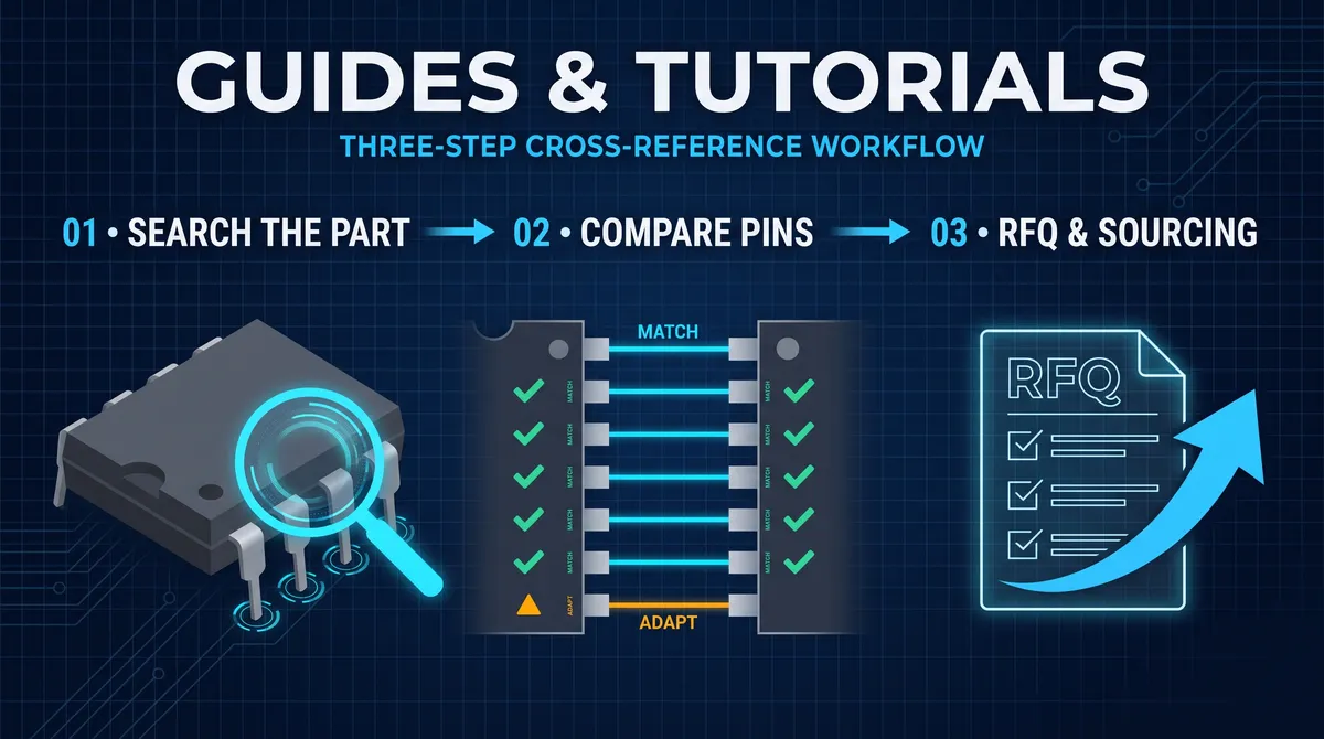
A shift register IC alternative is a companion question to the most common solution in digital I/O expansion, because the shift register is how a handful of microcontroller pins control a bus of outputs, and the 74HC595 is the part that nearly every build uses for the job. A shift register is a digital IC that moves data through a chain of stages on each clock edge, and the 74HC595 is the serial-in, parallel-out version that takes a stream of bits on one pin and presents them on eight output pins, which is how a user lights a row of LEDs, drives a display, or controls a bank of switches from three microcontroller pins. The alternatives question is easy to answer in one way, because the 74HC595's function is reproduced across a field of vendor parts and logic families, and harder in another, because the substitution has to respect the shift direction, the package, the supply, the speed, and the special features that this guide reads. This guide explains what a shift register does, how the 74HC595 fits, how to find its alternatives across the families, and how to substitute one safely, so that the output-expansion block on the board is chosen on the evidence.
The guide also covers the sibling that answers the reverse question, because not every shift-register need is a parallel-out one. The 74HC165 is the parallel-in, serial-out shift register, the part that reads a bank of buttons or switches into a stream of bits on one microcontroller pin, and its alternatives follow the same family structure as the 74HC595's. A designer who understands the two directions, the parallel-out for the driving and the parallel-in for the reading, understands the shift-register world, and this guide maps both. The shift register is one of the friendliest parts in the catalog to replace, because the function numbers and the pinouts are standardized across the families, and the guide gives the method that keeps the replacement safe, which is the same three-layer review this site's guides apply everywhere.
What a Shift Register Does and Why It Needs an Alternative
A shift register is a digital IC that moves its bit data through a chain of internal stages, one stage per clock pulse, and it exists in two useful directions that the world of I/O expansion lives on. The serial-in, parallel-out shift register, the 74HC595 and its kin, accepts a stream of bits on one serial input, shifts them through the register on the clock edges, and presents the current contents on a set of parallel output pins, which is how a handful of pins control many outputs, each output updated by shifting out a byte or a word. The parallel-in, serial-out shift register, the 74HC165 and its kin, captures the levels of a set of parallel inputs in one clock and shifts them out on one serial pin, which is how a controller reads many switches through few pins. The two directions are the two halves of the digital I/O expansion story, and both are built from the same shift-register architecture, which is why the same family logic and the same substitution method cover both.
The alternative question arises for the same reasons every part question does, the supply, the price, the end-of-life, and the second source. A design that uses the 74HC595 may need an alternative when the part is scarce, when the price of a specific vendor's part moves, when the design wants a logic family with different levels or speed, or when the sourcing needs two vendors on the same footprint. The shift-register world is well suited to the alternative because the function and the pinout are standardized, a 74HC595 from one vendor and a 74HCT595 from another and a domestic 74HC595 from a third share the function and the base pinout, so the substitution preserves the board. The alternative is the supply's answer, and the guide reads it through the family map, the specifications, and the verification, which is the honest way to substitute a part as standardized as the shift register.
The two shift-register directions: parallel-out and serial-out
The two shift-register directions answer two different I/O needs, and naming them prevents the classic substitution mistake. The parallel-out part, the 74HC595, receives serial data and drives eight parallel outputs, and it is the right part when the design needs to drive outputs, the LEDs, the display segments, the relay drivers, the indicator banks, from a few pins. The serial-out part, the 74HC165, reads eight parallel inputs and shifts them out serially, and it is the right part when the design needs to read inputs, the buttons, the switches, the encoder states, into a few pins. The two are not alternatives to each other, a 595 cannot read buttons and a 165 cannot drive outputs, and the substitution that mixes them fails at the function level before the datasheet review begins. The direction is the first fact of the alternative, and the designer reads it before the family, the package, or the speed.
The 74HC595 as the Shift Register Reference
The 74HC595 is the reference part for the serial-in, parallel-out shift register, and understanding it makes every alternative comparison concrete. The 74HC595 is an 8-bit serial-in, parallel-out shift register with an output latch, built in the high-speed CMOS logic family, and its architecture is the generator of the I/O-expansion world: the shift register shifts the serial data in on the clock, and the separate latch captures the register contents to the parallel outputs in one step, which lets the outputs update cleanly without the intermediate states flickering. The parts that follow the logic family and the supply, the HC family runs on the 2-to-6-volt CMOS supply with the CMOS input thresholds, and the part drives the outputs with the HC drive current, which is what lights the LEDs and drives the chips that need the stage of buffering. The 74HC595's popularity is the reason it is the reference, and the alternatives are read against it.
The 74HC595's package and pinout are also the reference the alternatives share. The part comes in the 16-pin package, the SOIC-16 and the DIP-16 and the TSSOP-16, with the serial data in, the shift clock, the latch, the output enable, the reset, and the eight parallel outputs on the standard pins, and the layout is reproduced across the vendor field and the logic families. The design that works with a 74HC595 reads the options that many of the family variants carry, the 74HCT595 with the TTL-compatible input levels for the 5-volt TTL world, the SOIC and the TSSOP packages for the footprint, and the vendor renumbers that carry the same function in the same pins. The reference part is the map's center, and the alternatives are its neighbors, which is the structure this guide uses to read the substitution.
How the 74HC595 expands I/O from a microcontroller
The 74HC595 expands a microcontroller's outputs by trading pins for time, and the trick is the shift register's architecture. The controller drives the serial data, the shift clock, and the latch, three pins, and shifts out the bits for the eight outputs, so the 595 turns three control pins into eight outputs, and two 74HC595s cascaded turn the same three pins into sixteen, and the chain grows with the register count. The output latch holds the driven levels steady while the next byte shifts behind it, which is why the 595 is the workhorse of the LED arrays, the seven-segment displays, the character displays, and the relay banks that the microcontrollers control. The expansion is the reason the part is everywhere, and the alternative question is, therefore, the question of replacing the workhorse without rebuilding the expansion. The 74HC595's place as the reference is the reason the alternative guide starts there, and the substitution method keeps the expansion intact.
The 74HC595 Family and Its Equivalents
The 74HC595 is the center of a family that the substitution reads as a map of equivalents. The first ring of the map is the logic-family versions, the 74HCT595 with the TTL-compatible input thresholds for the 5-volt board, and the other family grades where the vendor produces them, each carrying the same function and the same base pinout with the family's levels and speed. The second ring is the vendor field, the SN74HC595, the M74HC595, and the domestic 74HC595 parts, which reproduce the function and the pinout under their own prefixes, and which the sourcing can move between on the same footprint. The third ring is the functionally similar parts that share the shift-register job with a different feature set, the CD4094 with its enable and its different pinout, and the 74LS595 and the older grades, which require the pinout and the electrical check before the substitution. The map is the alternative's territory, and the design's board and the firmware decide which ring the alternative must come from.
The substitution within the family is the easy and the common move, and the substitution across the rings is the one that needs the check. A design that uses an SN74HC595 can source a domestic 74HC595 or a 74HCT595 on the same SOIC-16, changing the input thresholds where the HCT is involved, and the change is read against the driving microcontroller and the receiving loads. A design that moves to a CD4094 or a different-function part reads the pinout, because the features and the pins differ, and verifies the function the firmware expects, the latch, the enable, and the serial layout. The family map is the read that keeps the substitution fast where it is safe and careful where it is not, and it is the reason the 74HC595's alternatives are friendlier than most. The family standardization is the shift register's gift, and the verification is the discipline that spends the gift safely.
The 74HCT595 and other logic-family variants
The 74HCT595 and the other logic-family variants are the level-and-speed rings of the substitution, and reading them is a two-line check. The 74HCT595, the high-speed CMOS part with TTL-compatible input thresholds, runs on the 5-volt supply and accepts the TTL input levels that a bipolar TTL driver provides, so it is the choice when the 74HC595's CMOS thresholds would reject a TTL signal. The input threshold is the deciding specification, because a CMOS input at 5 volts requires a high above roughly 3.5 volts while a TTL input accepts a high above roughly 2 volts, and the design's driver decides which the receiver needs. The drive and the speed follow the family, and the substitution that changes the family changes the 595's behavior in the interface, so the designer verifies the levels and the drive against the driver and the load. The family variant is an easy alternative with a two-line check, and the check is what keeps the 74HC595's substitution clean.
Parallel-In Serial-Out Alternatives: The 74HC165 and Its Family
The reverse direction of the shift register, reading inputs instead of driving outputs, has the 74HC165 as its reference, and its alternatives follow the same family structure as the 74HC595's. The 74HC165 is an 8-bit parallel-in, serial-out shift register in the same HC logic family, the part that captures the levels of eight parallel inputs and shifts them out on one serial pin, and it is the workhorse of the button and switch reading across the microcontroller world. The alternatives ring around it the way they do the 595: the 74HCT165 and the other family grades for the levels, the vendor field of the SN74HC165 and the domestic parts, and the functional neighbors with their different features and pinouts. The selection between a 595-family part and a 165-family part is the direction decision, and the selection within the 165 family is the family-and-footprint decision, and the two decisions are the whole of the shift-register substitution.
The electronic design that reads many inputs through a shift register chooses the parallel-in part and the read path that the microcontroller runs, and the substitution of the 165 keeps the read path intact when the part and the family match. The 74HC165's function, to capture the parallel inputs and shift them on the clock, is standardized across the family, and the pinout and the package are reproduced on the SOIC-16 and the DIP-16, so the alternative that matches the family and the footprint preserves the board. The firmware that reads the inputs, the serial clocking and the load control, is agnostic to the vendor as long as the part behaves identically, which is the same property that makes the 595's substitution friendly. The 165's family is the mirror of the 595's, and the guide reads both directions under the same method.
How to choose between a 595-family and a 165-family part
Choosing between a 595-family and a 165-family part is a function decision, and the function decides before any specification. Use the serial-in, parallel-out 595 family when the design drives outputs, the LEDs, the displays, the drivers, and the indicator banks, because the parallel outputs are the point. Use the parallel-in, serial-out 165 family when the design reads inputs, the buttons, the switches, the encoders, and the sensor states, because the serial output to the controller is the point. A design that needs both, driving and reading, uses both families, a 595 chain for the outputs and a 165 chain for the inputs, and the two together are the complete I/O expansion. The choice between the families is not a performance contest, it is a direction requirement, and the designer who reads the direction first never substitutes a 165 for a 595 or the reverse. The direction is the first gate, and the family and the package are the second, and the two gates are the whole selection.
Key Specifications: Supply, Clock, Drive, and the Shift Register
The specification read of a shift register alternative covers the supply, the clock, and the drive, and it is the layer the family map does not fully state. The supply is the first: the HC family runs on 2 to 6 volts with the CMOS thresholds, the HCT family on the 5-volt TTL world, and the design's rail picks the family, because a 3.3-volt board uses the HC and a 5-volt TTL board uses the HCT where the levels demand it. The clock speed is the second: the maximum clock frequency and the propagation delay decide how fast the register shifts, and the design's update rate and the microcontroller's clock must fall inside the part's capability. The drive is the third: the output current the register can source and sink decides what the outputs drive, an LED needs the resistor and the current, and a relay driver needs the stage, and a lower-drive family changes the load design. The three specifications are the check against the board, and they are the reason a family variant is not a change to make without reading the datasheet.
The read also covers the special pins that the 74HC595 and its alternatives carry, and the features they enable. The output enable and the reset on the 595 control the outputs and the register, and the alternative must place the same functions on the same pins with the same behavior, because the firmware drives them. The latch, which separates the shifting from the output, is the feature that makes the 595 clean, and an alternative without the latch, or with a different latch behavior, changes the output update and the flicker that the design sees. The special features are part of the function, and the substitution verifies them rather than assuming the pin name is enough. The specification and the feature read is the datasheet layer of the alternative, and it is the layer that keeps a friendly substitution safe.
How to match the clock speed of a shift register alternative
Matching the clock speed of a shift register alternative is a matter of the headroom and the update rate. Read the maximum clock frequency of the alternative from the datasheet, and compare it against the clock the microcontroller actually drives, the SPI or the GPIO clock on the shift line, and leave the headroom, because the datasheet's maximum is the limit at the ideal conditions and the board's capacitance and the temperature reduce the real margin. Read the propagation delay that matters, the time from the clock edge to the output or the serial-out valid, and add it to the receiving circuit's timing where the design reads the chain, so the faster the chain the more the delays accumulate. A substitution that drops the maximum clock below the design's rate fails the shift, and one that raises the speed past the receiving firmware's expectation can break the read timing, so the match is a match of the headroom rather than of the number alone. The clock read is the timing discipline of the alternative, and it is the layer the bench test confirms.
Package Variants of the Shift Register
The package variants of the shift register are the footprint half of the alternative, and the SOIC-16, the DIP-16, and the TSSOP-16 cover the common boards. The SOIC-16 is the surface-mount standard, the DIP-16 the through-hole legacy for the prototypes and the breadboards, and the TSSOP-16 the compact surface-mount for the dense boards, and the alternative must match the footprint the board has laid out, because a board with an SOIC-16 pattern cannot mount a DIP-16 without the adapter. The package decision is separate from the function decision: a 74HC595 works in any of the packages, but the board chooses the one its footprint serves, and the substitution keeps the package constant while the function and the family are traded. The package variants also carry the pin pitch and the body size that the pick-and-place and the reflow read, and the substitution confirms the exact variant against the board rather than assuming the SOIC and the TSSOP are interchangeable. The package is the physical contract of the alternative, and the contract is the first fact of the substitution.
The SOIC-16, DIP-16, and TSSOP-16 footprints
The SOIC-16, DIP-16, and TSSOP-16 footprints are three different physical contracts for the same eight-bit function. The SOIC-16 carries the 16 leads on a standard body with a 1.27-millimeter pitch, the DIP-16 the through-hole leads on the 2.54-millimeter grid, and the TSSOP-16 the finer 0.65-millimeter pitch on the slimmer body, and a board designed for one does not mount the others. The alternative selection reads the board's footprint, sources the equivalent in that package, and keeps the pin map the same across the variants, because the function pins line up by the package convention. The prototype that started on a DIP-16 and the production that moves to an SOIC-16 or a TSSOP-16 follow the same function and the same firmware, with the package as the only change. The footprint comparison is the mechanical half of the alternative, and it is the half the schematic review resolves before the datasheet review begins.
When to Substitute a Shift Register and When Not
The substitution of a shift register is the right move within the family and the wrong move across the direction, and the guide's limit is the same as every substitution's. Substitute within the 74HC595 family, the vendor ring, the family grades, and the pin-compatible functional equivalents, when the supply or the price or the second source demands it, because the family map preserves the board and the firmware. Substitute within the 74HC165 family the same way for the input reading. Do not substitute across the direction, a 165 for a 595 or the reverse, because the function changes and the board that drives cannot read. And verify the special features, the latch, the enable, the reset, and the supply and the clock, against the board and the firmware before the volume, because the family map is the candidate list and the datasheet and the bench are the referees. The substitution is friendly because the family is standardized, and the limits are the direction and the features, which the method checks.
The response to a substitution limit is the same as every part: source, substitute, or redesign. Source the original where it is available, substitute the verified family member where the function and the footprint match, and redesign the block around a different part where the feature or the density demands it, recording the decision with the evidence. The shift register, being so standardized, rarely reaches the redesign, and the substitution is usually the answer, which is the honest friendliness of the category. The limit is the direction and the feature check, and the method that checks them is the method this guide provides, which is the same method this site's guides apply to every part it sources and replaces. The shift register's story is the standardized function and the deep family, and the substitution is the supply's friendliest answer.
Worked Example: Driving an LED Matrix with the 74HC595
Driving an LED matrix with the 74HC595 is the worked example that turns the shift register from a concept into a circuit, and the numbers are the design's first read. Take a row of eight LEDs on the eight parallel outputs, each with its series resistor, and the resistor value is the supply minus the LED forward drop divided by the desired current, so a 5-volt supply, a 2-volt LED, and a 10-milliamp target give a resistor of about 300 ohms, and the resistor both sets the brightness and protects the LED and the output. The microcontroller drives three pins, the serial data, the shift clock, and the latch, and the firmware shifts out a byte, one bit per clock, and then pulses the latch to move the register's contents to the parallel outputs in one step, which is how the outputs update cleanly without the intermediate states flickering. A byte of alternating ones and zeros lights every other LED, and the pattern is just the byte the firmware shifts. The worked example is the simplest face of the shift register, and it is the face that the cascades and the displays build on.
The example also reads the current that the outputs actually deliver, because the 74HC595's drive is the CMOS family's drive, in the milliamps rather than the hundreds of milliamps, so the LEDs drive through the series resistors and the heavier loads drive through the buffer stages. A bank of LEDs at 10 milliamps each draws 80 milliamps total from the supply but only a few milliamps through the chip's output pins after the resistors, and the display segments that need more current use the transistor or the driver stages that the design adds. The worked example shows the shift register as the control stage rather than the power stage, which is the correct mental model of the 74HC595's place, and it is the model the sourcing and the substitution both preserve, because an alternative that changes the drive changes the resistor and the load design. The LED matrix is the friendliest introduction to the shift register, and it is the introduction this guide uses to teach the rest.
A worked LED-resistor calculation for the 74HC595
A worked LED-resistor calculation for the 74HC595 is the small arithmetic that the example relies on. For a 5-volt supply, a 2-volt red LED, and a 10-milliamp target, the resistor is the supply minus the forward drop divided by the current, 3 volts divided by 0.01 amp, 300 ohms, and the standard 330-ohm value gives a slightly dimmer and safer 9 milliamps. For a 3.3-volt supply and the same LED, the resistor is 1.3 volts divided by 0.01, 130 ohms, and the standard 150-ohm value gives about 8.7 milliamps. The calculation scales with the LED color, a blue or a white LED drops more, and the design reads the forward voltage from the LED's datasheet rather than from memory, and it leaves the current below the LED's rating and the shift register's drive. The calculation is the first number of the LED example, and it is the number that the brightness and the longevity both depend on.
Cascading Two Shift Registers for 16 Outputs
Cascading two 74HC595 shift registers is the step from eight outputs to sixteen, and it is the pattern behind the larger displays and the bigger output banks. The cascade connects the serial output of the first register, the QH pin that passes the shifted-out bit, to the serial input of the second register, so the bit stream flows through both registers in one chain. The microcontroller shifts out sixteen bits, the first eight passing into the second register and the next eight filling the first, and then pulses the latch once, and both registers present their sixteen outputs in one clean update. The firmware shifts out the most-significant or the least-significant byte first depending on the order the design wants, and the order is the small detail that a mis-wired cascade shows as the LEDs landing in the wrong halves. The cascade multiplies the outputs without adding a single pin to the microcontroller, and it is the reason a handful of pins control a whole matrix of outputs, which is the shift register's defining value.
The cascade also reads the timing and the loading that the longer chain introduces. The clock that shifts the chain must drive both registers, and the clock's rise time and the propagation delay of the first register add a small delay to the second, which is well within the CMOS speeds at the typical update rates, and the serial path between the registers carries the data with no extra parts. The latch pulse updates both registers at once, so the sixteen outputs hold their state between updates without the glitch, and the supply bypass and the ground returns serve both parts. The cascade is the working proof of the shift register's expansion, and it is the pattern the sourcing view treats as a single block, because both registers come from the same family and the same substitution applies to both, which is the practical link between this section and the guide's replacement view.
Measuring and Troubleshooting the Shift Register
Measuring the shift register on the bench is the confirmation that the timing and the data path work, and it runs a short sequence. Probe the serial data, the shift clock, and the latch with the oscilloscope while the firmware shifts a known byte, and watch the data change on the clock edges, the latch pulse move the outputs, and the output pins present the pattern, and the measured timing against the firmware's shift rate confirms the circuit. Probe a single output pin while shifting a pattern that toggles it, to see the register's behavior cleanly, and probe the serial output of a cascade to see the data flowing to the second register. The measurement is the referee of the shift path, and the record, the waveform notes and the pattern check, is the evidence that the block works, which is the same discipline the series applies to every digital block.
The troubleshooting list for the shift register is short and consistent. If the outputs never update, check the latch, because a latch that is never pulsed holds the old outputs even when the register shifts, which is the most common miss of a first board. If the wrong LEDs light, check the bit order, the MSB-versus-LSB sequence that the firmware shifts, and the cascade connection, because a disconnected QH-to-serial leaves the second register unshifted and the pattern landing in the wrong half. If the outputs flicker or glitch, check the latch's separation from the shift, and if the outputs are dim, read the series resistors and the drive. If nothing at all appears, check the supply, the ground, and the clock, because a dead clock or a floating output-enable, which must be tied low, holds the outputs off. The troubleshooting list is the practical bookend to the worked example, and it is the checklist a designer keeps for the first shift-register board, on a single part and on a cascade alike.
The Firmware Side of the Shift Register
The firmware side of the shift register is the software half of the block, and the two implementation choices it makes are the hardware SPI and the bit-banged GPIO. The SPI hardware shifts the data automatically on the hardware clock, with the clock polarity and the phase set by the SPI configuration, and the firmware writes the byte and the peripheral clocks it out, which is the fast and the low-CPU path for a register that sits on the SPI bus. The bit-banged GPIO is the alternative, the firmware toggling the data and the clock pins directly, one bit per step, which works on any pin and any microcontroller but costs the CPU cycles, and the two are chosen by the platform and the update rate. The latch pulse, which moves the shifted data to the outputs, is the same in both, a GPIO toggled after the shift completes, and the latch's separation from the shift is the reason the outputs do not flicker as the bits flow through. The firmware side also reads the bit order, because the byte that lights the LEDs can be shifted most-significant or least-significant first, and the order is a convention the firmware and the wiring must agree on, which is the small software detail that the hardware troubleshooting often traces back to.
The firmware also owns the timing that the block depends on, because the shift clock and the latch must meet the register's timing and the design's update rate. A byte shifted at the firmware's loop rate updates the outputs at that rate, and the cascade shifts sixteen bits at the same rate, so the design reads the update rate against the application's need, a display that updates at 50 hertz versus a relay bank that updates rarely. The SPI hardware offloads the bit-shifting to the peripheral and the CPU is free, and the bit-banged version spends the cycles on every bit, which is the performance trade the firmware makes. The firmware side is the completion of the shift register block, and it is the half that the sourcing view inherits unchanged, because an alternative that matches the pins and the timing runs the same firmware, which is the practical link between the software and the replacement. The shift register is a hardware part driven by the firmware, and the two halves together are the block this guide has built from the pinout to the pattern.
Shift Register IC Alternatives: The Sourcing View
The sourcing view of the shift register alternative is the practical close, and it is the same discipline that the series has used. A design that standardizes on the 74HC595 or the 74HC165 selects a family that every vendor and the domestic manufacturers reproduce on the same footprint, so the sourcing can move across the vendor field and hold two suppliers on the same board, which is the second-source depth that the community has always used. The qualification of the alternative runs the same three-layer review, the package and the pinout, the supply, the clock, and the drive, and the special features, and the bench test across the temperature range, and the verified alternative is recorded beside the part in the BOM and the cross-reference. The shift register's standardization turns the alternative from a risk into a sourcing option, and the option is the value that the whole comparison delivers. A designer who reads the shift register IC alternative this way selects the family, the direction, and the verified vendor, and the selection is the working answer that the schematic, the firmware, and the board all accept.
Not sure which sensor fits your project?
Talk to our mmWave application engineers for a free consultation.
Specify your hotel project with our engineers
Send your room count, ceiling type, and protocol preference. We will return a sample plan and quote within 24 business hours.
- Move from general guidance into a product or application discussion.
- Use RFQ when pricing, drawings, MOQ, or launch timing needs structure.
- Keep a direct contact path visible for fast clarifications and handoff.