Pin-Compatible Microcontroller Replacement Guide
Pin-compatible microcontroller replacement guide: how to check the pinout, register map, and firmware compatibility of an MCU alternative and qualify the swap.
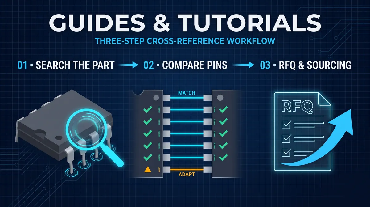
A pin-compatible microcontroller replacement is an MCU that fits the same pinout and package as the original, so it mounts on the same board, and for most engineers the harder half of the question is whether it also runs the same code. Unlike a regulator or a logic chip, a microcontroller carries a second compatibility layer, the firmware, and a part that matches every pin can still fail the project if its core, its register map, or its peripherals differ from the original. The microcontroller world nonetheless has the most active pin-compatible replacement market in electronics, because a dominant device like the STM32F103 defines a pinout that a field of manufacturers reproduces, with domestic makers building pin-compatible and largely code-compatible parts that are qualified against the same board. This guide explains the two compatibility layers, how the STM32 ecosystem works as the working example, how to check the pinout and the register map, how to run the firmware bring-up that qualifies the swap, and when the replacement is not enough, so that a pin-compatible microcontroller replacement is a documented engineering decision rather than a bench gamble.
The reason microcontroller replacement deserves its own guide is that the failure modes are invisible to a pinout check. A replacement that shares the LQFP48 package and the pin names can differ in the ADC resolution, the timer features, the DMA channels, the boot pins, or the clock tree, and the differences surface as firmware bugs, missing peripherals, and intermittent failures at temperature. The qualification is therefore a three-layer review plus a firmware bring-up: the physical pins, the electrical parameters, the register and peripheral compatibility, and then the compiled and running firmware on a reference board. The good news is that the manufacturer migration notes and the compatibility matrices exist for exactly this purpose, the STM32-to-GD32 path is documented, and a buyer who reads them qualifies an MCU alternative in days rather than in months. This guide turns that path into a method, and it is the method this site's engineers apply to every microcontroller replacement they ship.
What Pin-Compatible Microcontroller Replacement Means
A pin-compatible microcontroller replacement is an MCU that places the same pins on the same package as the original, and the term has a precise engineering meaning that the replacement practice is built around. The package must match, an LQFP48 replacement for an LQFP48 original, and the pinout must match, the power pins, the ground pins, the oscillator pins, the reset, the debug pins, and every GPIO and peripheral pin carrying the same function on the same position, so the board mounts the replacement without re-layout. The pin compatibility is the physical layer, and it is necessary but not sufficient, because a microcontroller's value is in what the firmware makes it do, and the firmware runs on the core, the register map, and the peripherals that the pinout does not reveal. A pin-compatible replacement therefore has to be judged on both layers, and the second layer, the code compatibility, is the one that decides most MCU swaps in the end. The practice of pin-compatible replacement is the combination of the two layers, the part that fits and the part that runs, and the guide treats both with the same weight.
The two layers also define the two kinds of MCU alternatives that the market offers. A pin-compatible alternative matches the pins and the package, and it may or may not match the code, so a board can mount it but the firmware may need porting. A pin-and-code-compatible alternative matches the pins and aims for software compatibility, the same core family, the same register map, and the same peripheral behavior, so the firmware compiles and runs with little or no change, and it is the higher-value form. The domestic manufacturers of the STM32 ecosystem build the second form, the GD32 and the AT32 families that are not only pin-compatible but register-and-instruction compatible enough to run much of the original firmware. The buyer's question is always which form the candidate is, pin-only or pin-and-code, and the answer decides the qualification's cost, the pin-only candidate demands a porting effort, and the pin-and-code candidate demands a verification effort. The guide checks the form before the qualification, and the form is the first fact of every MCU replacement.
Why microcontrollers need a code layer that other ICs do not
The code layer exists because a microcontroller is a programmable device, and the program it runs is as much a part of the design as the pins. A regulator's replacement is judged by its electrical behavior, and a logic chip's by its function, but an MCU's replacement is judged by whether the stored firmware, the compiled binary that the original part executed, runs correctly on the candidate. The firmware depends on the core architecture, the instruction set, the flash and the SRAM sizes, the register map of the peripherals, the clock tree, the interrupt controller, and the boot behavior, and a difference in any of them shows up as a compiled binary that does not run, a peripheral that does not respond, or a timing that drifts. The code layer is the reason an MCU replacement cannot be approved on the pinout alone, and it is the layer that the firmware bring-up test exists to verify. The buyer and the engineer who understand the code layer read the migration notes and the register maps before the pins, because the code is the part of the MCU that the board actually uses, and the code compatibility is the difference between a replacement and a project.
The STM32 Ecosystem and Its Pin-Compatible Alternatives
The STM32 ecosystem is the working example of pin-compatible microcontroller replacement, because it is the family with the most documented alternatives and the most active replacement market. The STM32F103, the classic Cortex-M3 part that powered a generation of boards, defines an LQFP48 pinout that a field of devices shares, and the migration and the compatibility documents state which devices are pin-compatible and which code changes the swap implies. The domestic manufacturers built the most interesting layer of the ecosystem: GigaDevice's GD32F103 and the GD32 family, Artery's AT32F403A, and the wider field of domestic Cortex-M and pin-compatible parts, which target not only the pins but the software, with the register maps and the driver ecosystems designed to accept the STM32 firmware with limited porting. The ecosystem is the reason the phrase pin-compatible microcontroller replacement names a practical market rather than a theoretical possibility, and it is the reason a buyer with an STM32-based design has real alternatives when the STM32 is scarce, priced up, or end-of-life.
The ecosystem also shows the two layers in action, and the compatibility matrix is the document that maps them. ST's own datasheets and the family migration guides state which devices share the pinout, the flash, and the peripheral set, and the domestic manufacturers publish their own compatibility tables stating which STM32 devices their parts replace and what the differences are. The matrix is the starting point of every replacement, because it names the candidate, the compatibility level, and the differences before the datasheet review begins. The buyer reads the matrix for the exact device on the board, the STM32F103C8T6 and its pin-and-code-compatible candidates, and then verifies the matrix against the actual firmware and the actual board, because the matrix is a claim that the bring-up test confirms. The ecosystem is the map, the matrix is the route, and the bring-up is the proof, and the three together are the method that this guide applies to every MCU replacement.
The GD32 and AT32 alternatives to the STM32
The GD32 and the AT32 families are the best-known pin-compatible alternatives to the STM32, and knowing their shape helps a buyer read the ecosystem. GigaDevice's GD32F103 mirrors the STM32F103's LQFP48 pinout and targets software compatibility with the Cortex-M3 core, the same flash and SRAM ranges, and a register map designed to run STM32 firmware with limited porting, and its family extends the pattern across the GD32 lineup. Artery's AT32F403A and the AT32 family take a similar approach, with pin-compatible parts that aim for the same software compatibility and add their own performance and feature variations. The alternatives are not guaranteed identical, the ADC, the timers, the clock tree, and the peripheral register maps can differ in details that the firmware uses, and the differences are exactly what the migration note and the bring-up test surface. The buyer who qualifies a GD32 or an AT32 reads the compatibility matrix, compares the peripheral map the firmware actually uses, compiles and runs the firmware on the candidate, and tests across the temperature range. The alternatives are the market's answer to the STM32's scarcity and price, and the qualification is the discipline that makes the answer safe.
How to Check Pin Compatibility for a Microcontroller
The pin compatibility check for a microcontroller is the same three-layer review as any substitution, run at the MCU's scale. Confirm the package first, the LQFP48, the QFP64, or the BGA, and the exact package suffix, because the package decides the footprint and the MCU's pin count is fixed by the package. Compare the pinout second, pin by pin, the power and the ground pins, the oscillator pins, the reset and the boot pins, the debug and the test pins, and every GPIO and peripheral pin, using the pin diagrams from the two datasheets, and record each pin's function in a table with the match verdict. Confirm the pin functions third, because a pin that is an alternate function on the original may be a GPIO-only or a differently multiplexed pin on the candidate, and the firmware that uses the alternate function has to find it on the same pin. The pin compatibility check is exhaustive because the MCU's pins carry many functions through the multiplexer, and a single functional pin that differs, a boot pin, a VBAT pin, or an ADC channel, can break the swap that the package matching promised.
The pin check also reads the multiplexing and the alternate functions, which is the MCU-specific layer that a simple part does not have. A microcontroller pin carries a primary function and a set of alternate functions through the pin multiplexer, and the firmware assigns the alternate functions in the registers. The pin-compatible candidate must place the alternate functions the firmware uses on the same pins, the USART, the SPI, the I2C, the timer channels, and the ADC channels, and the comparison reads the alternate function tables of the two parts. The comparison is where the GD32 and the STM32 differ in the details, and where the migration notes are worth their weight, because the notes state which alternate functions moved and which registers changed. The pin compatibility of a microcontroller is therefore a package check, a pin check, and a multiplexing check, and the three together are the first layer of the replacement qualification. A candidate that passes the three is physically compatible, and the code layer decides the rest.
How to read an MCU pinout diagram for replacement
Reading an MCU pinout diagram for replacement is a disciplined comparison, and it runs on a few reliable habits. Place the two pin diagrams side by side, numbered from pin 1, and walk the perimeter in order, checking every pin's function against the original. Mark the power and the ground pins first, then the oscillator, the reset, and the boot pins, then the debug pins, and then the GPIO and the peripheral pins, and record each in the table with the match, the mismatch, or the power-only verdict. Read the alternate function tables for the pins the firmware uses, and confirm the alternate function lives on the same pin on the candidate. Read the package suffix, because the LQFP48 and the QFP48 and the TQFP48 are not automatically the same footprint, and confirm the body and the pin pitch against the board's pad geometry. The habit produces the pin compatibility table that the change record needs, and it is the table that turns the candidate's claim into the buyer's evidence. A pinout comparison done this way takes an hour for an MCU, and it catches the swaps that the package matching misses, which is the value of the discipline.
How to Check Code and Register Compatibility for a Microcontroller
The code compatibility check is the layer that decides most MCU replacements, and it runs in three parts that the firmware's behavior dictates. The first part is the core and the instruction set, confirming that the candidate's core, the Cortex-M3, the Cortex-M4, or the other, matches the original's, and that the instruction set and the toolchain the firmware was built with are supported, because a different core architecture changes the compiled binary at the instruction level. The second part is the memory map, confirming the flash and the SRAM sizes meet the firmware's needs, and the base addresses and the boot memory layout match the linker script, because a firmware that expects the original's memory map crashes on a different one. The third part is the peripheral and the register map, confirming the peripherals the firmware uses, the clock tree, the GPIO, the timers, the USART and the SPI, the ADC, the DMA, and the interrupts, exist on the candidate with the same registers and the same behavior. The three parts are read from the migration notes and the register maps, and they are the code layer's datasheet, the document that states what the firmware can expect.
The register compatibility is the fine print of the code layer, because the firmware reads and writes the registers directly, and a register that moved, changed meaning, or does not exist breaks the code that touches it. The comparison reads the register map of each peripheral the firmware uses, the clock control, the GPIO, the timers, the communication peripherals, the ADC, and the DMA, and it confirms the registers, the bits, and the behaviors match the original. The migration notes state the differences, the registers that changed, the peripherals that differ, and the driver changes the swap implies, and they are the authoritative source because the manufacturer owns the silicon. The register comparison is the bridge between the datasheet and the firmware bring-up, because it predicts where the bring-up will fail, and the bring-up confirms where the prediction was right. A candidate whose register map matches the firmware's usage is code-compatible on paper, and the bring-up test is the proof that it is compatible in the running code.
How to compare the peripheral map the firmware actually uses
Comparing the peripheral map is a matter of knowing what the firmware actually touches, and the knowledge comes from the code rather than from the datasheet. List the peripherals the firmware initializes and drives, the clocks, the GPIO ports and pins, the timers and their channels, the USART, SPI, and I2C, the ADC channels, the DMA, the interrupts, and the watchdog, and for each, list the registers the code reads and writes. Compare the candidate's register map for each peripheral against the original, and flag the registers and the bits that differ, the timers with a different number of channels, the ADC with a different resolution or channel mapping, and the DMA with a different request map. The comparison is the map of the porting effort, because the peripherals that match need no work, the peripherals that differ need the driver change, and the peripherals that do not exist need the redesign. The peripheral map comparison is the professional's answer to the code layer, and it is the reason a buyer can estimate the porting cost of a pin-only candidate before the bring-up begins. The map turns the firmware from a black box into a checklist, and the checklist is what the bring-up test executes.
Firmware Bring-Up: The Real Qualification of an MCU Replacement
The firmware bring-up is the test that qualifies an MCU replacement, and it is the step that the datasheet and the register review cannot replace. The bring-up runs in stages, each building on the last. The first stage is the toolchain, confirming the compiler, the linker, the debugger, and the device pack accept the candidate and build the firmware for its core. The second stage is the boot and the clock, programming the candidate and confirming it boots, its reset vector, its startup code, and its clock tree produce the expected clocks. The third stage is the peripheral bring-up, exercising every peripheral the firmware uses, the GPIO, the timers, the USART and the SPI, the ADC, the DMA, and the interrupts, and comparing the behavior and the timing against the original device. The fourth stage is the system test, running the full firmware in the actual application, and the fifth is the soak, running the product across its operating voltage and temperature range to surface the intermittent differences. The bring-up is the referee of the whole replacement, and a candidate that passes it is a replacement, while one that fails it is a porting project or a non-starter.
The bring-up also produces the evidence that the replacement needs, because the qualification is only as good as its record. Record the toolchain result, the boot and the clock measurements, the peripheral bring-up results, the system test pass, and the soak test log, beside the original device's measurements, and keep the record with the change note. The record is what an ISO-managed process accepts and what a single-engineer shop values even more, because it turns the replacement from a bench event into a documented decision. The bring-up also sets the timeline, because a pin-and-code-compatible candidate with a clean peripheral map can bring up in days, while a pin-only candidate with a divergent map takes the porting weeks. The timeline is the economic fact of the replacement, and it is the reason the buyer reads the peripheral map before the bring-up, to know which candidate deserves the days and which deserves the weeks. The bring-up is the qualification's heart, and the record is its voice.
How to run a bring-up test on an MCU replacement
Running a bring-up test on an MCU replacement is a staged procedure that a lab can run in a repeatable order. Start with the toolchain, install the candidate's device support in the IDE, and build the original firmware against the candidate, fixing the startup and the clock configuration errors that the compiler surfaces. Flash the candidate on the reference board, and confirm the boot, the reset, the debug connection, and the clock outputs, using the oscilloscope and the debugger. Exercise the peripherals the firmware uses, one by one, driving the GPIO, the timers, the serial ports, the ADC, and the DMA, and compare the waveforms and the values against the original device. Run the full application, and confirm the product's function end to end. Then soak the board across the voltage and the temperature range the product sees, and log the failures. The staged procedure isolates each difference as it appears, and it produces the evidence that the replacement passes or the list of what it needs. A bring-up that reaches the soak test with no differences is the completion of the qualification, and a bring-up that fails at a stage is the start of the porting decision.
Peripheral and Analog Differences That Break the Swap
The differences that break a pin-compatible MCU replacement are the ones the pinout check cannot see, and the analog and the peripheral details are the first place they live. The ADC is the classic example: a candidate with the same pins can have a different resolution, a different channel mapping, a different reference, or a different conversion timing, and the firmware that reads a specific channel on a specific pin with a specific resolution breaks or drifts on the candidate. The clock tree is another: a candidate with the same crystal pins can have a different PLL configuration, a different clock source, or a different max frequency, and the firmware that derived its baud rates and its timers from the original clocks runs wrong on the candidate. The timers and the PWM, the communication peripherals and their FIFO and DMA behavior, and the boot and the debug pins, each carry details that differ across a pin-compatible field. The differences are the reason the peripheral map comparison and the bring-up test are the core of the qualification, and the buyer who skips them approves a swap that works on the bench and fails in the field.
The analog differences deserve their own caution, because they are the quietest failures. The ADC noise and the linearity, the reference voltage, the input impedance, the comparator behavior, and the power supply rejection differ across manufacturers and across silicon revisions, and a design that relied on the original's analog behavior sees the differences as measurement error, threshold drift, or noise. The operational amplifiers and the comparators inside an MCU, where the part has them, and the DAC and the analog switches, all carry the same risk. The qualification of the analog path is the comparison against the original's measured behavior, not against the datasheet alone, and it is the soak test across the temperature and the supply that surfaces the drift. The analog differences are the reason the bring-up runs the actual product test and the temperature pass, and the buyer who treats an MCU replacement as a digital-only swap imports the analog risk that the datasheet never promised.
How to compare ADC and timer behavior on an MCU replacement
Comparing the ADC and the timer behavior on an MCU replacement is a measurement exercise, and it runs on the actual board. For the ADC, configure the candidate's ADC exactly as the firmware does, the resolution, the channel, the reference, and the sampling, read a known voltage, and compare the code, the linearity across the range, the noise, and the settling against the original device. For the timers, configure the candidate's timer as the firmware does, the prescaler, the period, the compare values, and the channels, and measure the frequency, the duty, the jitter, and the trigger behavior against the original. For the PWM, the input capture, and the dead-time where the design uses them, run the same comparison. The measurements are recorded beside the original's, and the differences, a bit of ADC offset, a timer period drift, or a PWM edge jitter, are judged against the product's tolerance. A candidate whose ADC and timers match the original within the product's tolerance is qualified, and one whose behavior drifts beyond it needs the driver change or the redesign. The measurement comparison is the referee of the peripheral layer, and it is the evidence that the bring-up test produces.
Worked Example: Porting a UART and GPIO Firmware to the Alternative
Porting a UART and GPIO firmware to the alternative is the worked example that shows the code layer in practice, and a firmware that uses the GPIO and a UART at 115200 baud covers the typical ground. The toolchain step adds the alternative's device pack and the startup to the project, and the firmware builds against the alternative's device definition, with the compiler and the linker surfacing the differences first. The clock step ports the system-clock configuration to the alternative's clock registers, because the PLL scheme differs in the register layout, and the measured system clock on the output pin confirms the port. The peripheral step ports the GPIO and the UART to the alternative's library, and the UART is instructive, because the baud-rate register computes differently and the ST value copied over produces a garbled stream, so the 115200 configuration is re-derived from the alternative's calculation and confirmed on the wire with a terminal. The application step runs the existing loop, the GPIO toggles and the UART transmits as the original did, and the bring-up record, the compile, the clock, the peripherals, and the application, is the evidence the swap is qualified. The worked example is the model for the firmware layer, and it is the model the peripheral-map section set up.
The worked example also reads the order that makes the port fail less, because the toolchain before the clock, the clock before the peripherals, and the peripherals before the application is the order that localizes the failures as they appear. A port that builds first and verifies each stage before the next turns a chain of surprises into a sequence of confirmed stages, and the record of each stage is the evidence the change control accepts. The worked example is the concrete face of the code layer, and it is the face that the bring-up section of this guide formalizes, which is the practical completion of the MCU replacement method.
Peripheral Bring-Up: A Worked Sequence for the ADC
The peripheral bring-up sequence for the ADC is the worked example that shows the analog layer of the MCU swap, and it is the place where a pin-clean replacement often fails. Configure the alternative's ADC exactly as the firmware does, the resolution, the channel, the reference, and the sampling, and read a known voltage, comparing the code, the linearity across the range, the noise, and the settling time against the original device's readings. A candidate whose ADC configures differently, a channel map that moved, a reference that differs, or a resolution that changed, shows the difference in the read values, and the porting adjusts the configuration and the firmware driver. The measurement, the codes at the known voltages, the noise, and the settling, is the record that the ADC layer is qualified, and it is the record that the analog-soak section builds on. The ADC bring-up is the model for every peripheral that the firmware drives, the timers, the serial ports, the DMA, and the interrupts, and it is the model that turns the peripheral map from a list into a verified behavior.
The ADC bring-up also reads the temperature behavior, because the analog layer drifts across the range in a way the digital layer does not. Run the ADC read across the product's temperature, and compare the drift against the original and against the product's tolerance, because a candidate whose ADC drifts past the tolerance at the high or the low end is a candidate the soak test rejects. The ADC bring-up's temperature pass is the reason the qualification runs the product's range rather than the bench's happy path, and it is the reason the analog layer is tested on the board rather than on the datasheet. The worked ADC sequence completes the bring-up half of the MCU replacement, and it is the half that the workflow's final stages execute, which is the practical close of the method.
When a Pin-Compatible MCU Replacement Is Not Enough
The honest limits of MCU replacement are the cases where the pins and the code cannot save the design, and knowing them prevents a wasted qualification. The first limit is the genuine feature gap: a candidate with the same pins and a similar register map can still lack a peripheral, a feature, a core, or a performance level the firmware requires, an ADC with a lower resolution, a timer with fewer channels, a USB peripheral with a different implementation, or a core too slow for the workload, and the gap forces a porting or a redesign regardless of the pins. The second limit is the certified or the approved part: an MCU under an agency approval, a functional safety classification, a medical or an aerospace qualification, or a security certification is not interchangeable with a pin-compatible alternative unless the alternative carries the same certification, and the certification is per-device, not per-pinout. The third limit is the vendor-specific dependency: a firmware stack that relies on a manufacturer's library, a driver, an encryption unit, or a debug tool that the candidate does not support forces a porting effort that can exceed the redesign's. Each limit is read before the qualification rather than discovered after, and the reading is the same datasheet and matrix review the method always runs.
The response to the limits is the response to every substitution: source, substitute, or redesign. Source the original when it is still available, through the authorized channel and the independents. Substitute the pin-compatible and code-compatible alternative when the pins, the registers, and the firmware qualify, and document the bring-up. And redesign around a current MCU when the feature gap, the certification, or the dependency rules the alternative out, with the full engineering pipeline and the transition plan. The decision is recorded with the evidence, the matrix, the peripheral map, the bring-up record, and the certification check, so the next review sees the reasoning. A pin-compatible MCU replacement program that knows its limits is a program that swaps the parts that can be swapped and plans the parts that cannot, and the limits are the boundary of the pinout's power, respected by the engineer who reads the code layer before believing the pins.
A Workflow for Pin-Compatible Microcontroller Replacement
The full method fits into a workflow that an engineer and a buyer run in the same order. First, capture the original, the exact device, the package, the flash and the RAM, and the firmware it runs, and pull the datasheet and the migration notes. Second, screen the candidates, the compatibility matrix and the cross-reference, the GD32, the AT32, and the field, and read which candidates are pin-compatible and which are pin-and-code-compatible. Third, check the pins, the package, the pinout, and the alternate functions, and build the pin table. Fourth, check the code, the core, the memory map, the peripheral map, and the registers the firmware uses, against the migration notes, and estimate the porting effort. Fifth, bring up the candidate, the toolchain, the boot, the peripherals, the system test, and the soak, and record the measurements beside the original. Sixth, decide, the source, the substitute, or the redesign, on the evidence of the bring-up and the certification, and record the decision. Seventh, manage the transition, the pilot, the ramp, and the legacy stock, and update the BOM and the cross-reference. That sequence is the pin-compatible MCU replacement method, and it is the same method whether the original is an STM32F103, a GD32, or any other device in the field.
The workflow is the reason a pin-compatible microcontroller replacement is a manageable, documented engineering activity rather than a bench gamble. With the matrix screened, the candidates are known. With the pins checked, the board is preserved. With the code checked, the porting effort is estimated. And with the bring-up run, the replacement is proven in the running firmware, not just on the datasheet. The entire value of the method is that the most consequential substitution in electronics, the one that carries firmware, timing, and analog behavior with it, is handled with the same two-layer review and the same evidence discipline as the simplest part swap, and that discipline is what turns the STM32 ecosystem's alternatives into a working supply option. A team that runs this workflow qualifies a pin-compatible microcontroller replacement with a pin table, a peripheral map, and a bring-up record, which is the entire point of an MCU replacement done right.
Not sure which sensor fits your project?
Talk to our mmWave application engineers for a free consultation.
Specify your hotel project with our engineers
Send your room count, ceiling type, and protocol preference. We will return a sample plan and quote within 24 business hours.
- Move from general guidance into a product or application discussion.
- Use RFQ when pricing, drawings, MOQ, or launch timing needs structure.
- Keep a direct contact path visible for fast clarifications and handoff.