NE555 vs NE556: Which Timer IC Do You Need
NE555 vs NE556: compare the single 555 timer and the dual 556 timer by package, pinout, supply, timing, and when to choose each for your circuit.
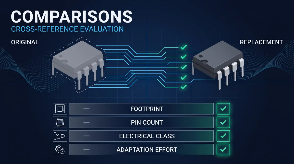
NE555 vs NE556 is a comparison every timer user makes when the design needs more than one timing circuit, and it is one of the cleanest comparisons in electronics because the two parts share the same internal timer. The NE555 is a single timer IC, one complete timing circuit in an 8-pin package, and the NE556 is a dual timer IC, two independent copies of the same 555 circuit in a 14-pin package, and the two deliver the same monostable and astable behavior on the same supply and timing specifications. The comparison is therefore about the count and the package: a design that needs one timing circuit takes the NE555, and a design that needs two takes the NE556 and saves the board a second part. This guide compares the two across the package and the pinout, the supply and the timing, the monostable and the astable operation, and the applications, and it gives the rule for choosing between them, so the timer block picks the single or the dual on the evidence.
The comparison also opens the replacement view, because the 555 and the 556 sit in one of the most widely reproduced families in electronics. The NE555's 8-pin layout is shared by the LM555, the SA555, the SE555, the TLC555 and the CMOS 555 variants, and the NE556's 14-pin layout is shared across the same field, so a design that chooses either part has a deep, pin-compatible replacement market. The guide therefore covers the engineering comparison and the sourcing view together, and it is the working reference an engineer keeps beside the two datasheets. The NE555 and the NE556 are the same timer in two package counts, and the comparison is the map between the single circuit and the dual.
NE555 vs NE556: The Core Difference
The core difference between the NE555 and the NE556 is the number of timing circuits in the package, and every practical difference follows from the count. The NE555 contains one complete 555 timer, the trigger, the threshold, the discharge, the control, the reset, and the output, in an 8-pin package, and the NE556 contains two complete and independent 555 timers in a 14-pin package, each with its own trigger, threshold, discharge, control, reset, and output pins. The two timers inside the NE556 are the same design as the single NE555, they run from the same supply, and they produce the same monostable and astable behavior, so the comparison is not a performance contest, it is a packaging and a count decision, how many timing circuits the board needs and which package serves them. The engineer who understands that reads the rest of the comparison correctly, the single for the one-timer design and the dual for the two-timer design.
The two parts also share the timing architecture that defines the family, and the shared architecture is worth stating because it explains every specification that follows. A 555 timer works by comparing a capacitor voltage against two internal references, the lower trigger reference at one-third of the supply and the upper threshold reference at two-thirds of the supply, and it drives an internal discharge transistor and an output stage from the comparison. The monostable mode triggers the timer for a single output pulse whose width is set by an external resistor and capacitor, and the astable mode makes the timer oscillate continuously with the frequency and the duty set by two external resistors and a capacitor. The NE555 and the NE556 are the same architecture in one and two copies, and the comparison of the timing, the supply, and the output is a comparison of the shared design. The core difference is the count, and the shared architecture is what the count multiplies.
The single 555 timer versus the dual 556 timer
The single and the dual timers differ in exactly one dimension that matters to the schematic, the number of timing circuits the board can use. A design that needs one oscillator, one one-shot, one pulse generator, or one delay, takes the NE555 and uses a single 8-pin part, and a design that needs two of any of those, an oscillator and a one-shot, two delays, or two oscillators, takes the NE556 and uses one 14-pin part for both. The NE556 is not a faster or a better timer than the NE555, it is two of the same timer, and the comparison that pits them as rivals misses the point, they are the same circuit in two package counts. The dual also carries the shared-supply convenience, the two timers run from the same VCC and ground and the designer bypasses the supply once, and it carries the shared-temperature character, the two timers track each other as the temperature moves. The single-versus-dual difference is the count, and the count decides the package, and the package is what the board mounts.
Pinout and Package: NE555 vs NE556
The package and the pinout are the physical difference the board cares about, and the comparison is a footprint decision. The NE555 comes in the 8-pin package, the DIP-8 and the SOIC-8, with its pins arranged as ground, trigger, output, reset, control, threshold, discharge, and supply, and the design that uses one timer reads the 8-pin layout. The NE556 comes in the 14-pin package, the DIP-14 and the SOIC-14, with timer A occupying one half of the pins and timer B the other, sharing the supply on the end pins, and the design that uses two timers reads the 14-pin layout. The two packages are not interchangeable, a board that mounts an NE555 cannot mount an NE556, and a board that needs two timers does not want two NE555s when one NE556 serves the job in less space. The package decision is the first decision of the comparison, and it is the decision the schematic and the layout follow.
The pinout also carries the pin functions that the designer wires, and the comparison reads them per timer. The NE555's eight pins carry the trigger, the output, the reset, the control voltage, the threshold, and the discharge, and the NE556's two timers carry the same functions on their own pins with the supply shared, and the timing circuit the designer builds for an NE555 translates directly to either half of an NE556 by mapping the pins. The reset and the control pins deserve their read, because the reset overrides the timing and the control pin sets the timing references, and the design that uses them wires them the same way in both parts. The package and the pinout are the physical contract of the comparison, and the pin functions are the contract's fine print, and the designer who reads them wires the single or the dual with the same timing circuit.
The NE555 8-pin and NE556 14-pin layouts compared
Comparing the 8-pin and the 14-pin layouts places the single timer and the dual timer side by side. The NE555's 8-pin layout walks the timer's pins around the package, the supply at pin 8, the ground at pin 1, and the trigger, the threshold, the discharge, the control, the reset, and the output across the middle, while the NE556's 14-pin layout gives timer A the pins on one side and timer B the pins on the other, with the supply at one end and the ground at the other. The board designer reads the layout as a footprint, the SOIC-8 pad pattern and the SOIC-14 pad pattern are distinct, and the selection is locked to the layout the schematic draws. The layout also reads the noise and the cross-talk story, because two timers in one package share the substrate and the supply, and the design that runs both timers at the same time bypasses the supply and separates the ground paths the way the datasheet's layout note recommends. The layout comparison is the physical half of the selection, and it is the half the schematic resolves first.
Supply and Timing Specifications: NE555 vs NE556
The supply and the timing specifications of the NE555 and the NE556 are the same per timer, because the timers are the same design, and the comparison reads them as shared rather than as differences. Both parts run on a supply from roughly 4.5 volts to 16 volts, the classic bipolar 555 range, and both draw the operating current that the datasheet lists, with the NE556 drawing the current for its two timers and the NE555 for its one. The timing behavior is the same: the monostable output pulse is about 1.1 times the external resistor times the capacitor, and the astable frequency and duty are set by the two external resistors and the capacitor with the classic 0.693 factors, and the accuracy of the timing depends on the external components and the temperature rather than on which of the two parts runs the circuit. The supply and the timing are the shared ground of the comparison, and the designer who knows the 555 timing formulas knows the 556, because the two halves of the 556 run the same formulas.
The timing specifications also carry the limits that the design reads, because the family's accuracy is the story of the 555. The threshold and the trigger levels track the supply at one-third and two-thirds, which is why the 555's timing is supply-ratio based rather than absolute, and the accuracy of a 555 monostable or astable circuit is set by the external resistor and capacitor tolerances and the timer's own internal reference accuracy, a few percent typical for the classic part. The output drive and the sink are the same per timer, the classic bipolar output that can source and sink the tens of milliamps that the datasheet specifies, and the supply range and the output are the design's interface to the load. The comparison of the supply and the timing is the comparison of the shared design, and the NE555 and the NE556 are equally capable at the same supply and the same timing, which is the honest statement the datasheet makes.
How the timing formulas apply to both timers
The timing formulas apply identically to the NE555 and to each half of the NE556, because the internal architecture is the same. In the monostable mode, a trigger on the trigger pin starts an output pulse whose width is approximately 1.1 times the timing resistor times the timing capacitor, and the formula holds for the single timer and for either timer of the dual. In the astable mode, the output oscillates with the charge time set by the sum of the two resistors through the capacitor and the discharge time set by the lower resistor, with the frequency and the duty computed from the classic 0.693 factors, and again the formula holds for both parts. The design that builds a one-shot with an NE555 builds the same one-shot with either half of an NE556 by mapping the pins and the external resistor and capacitor, and the timing is the same within the component tolerances. The shared formulas are the reason the comparison of the timing is a comparison of the same numbers, and they are the reason a designer fluent in the 555 is fluent in the 556.
Monostable and Astable Operation: NE555 vs NE556
The two operating modes of the 555 family are the monostable, the one-shot, and the astable, the oscillator, and the comparison of the NE555 and the NE556 is a comparison of the same modes in one and two copies. The monostable mode produces a single output pulse when triggered, used for the debounce, the delay, the timed pulse, and the one-shot sequences, and the NE555 serves one monostable while the NE556 serves two, two delays, a delay and a pulse, or a pair of sequences. The astable mode produces a free-running oscillator, used for the blinkers, the tone generators, the PWM, the clock sources, and the pulse trains, and the NE555 serves one oscillator while the NE556 serves two, two frequencies, an oscillator and a one-shot, or a variable and a fixed pulse. The modes are the family's vocabulary, and the count decides how many of the vocabulary the board uses, which is the comparison's practical core. The design that needs one mode in one place takes the single, and the design that needs two modes or two of one mode takes the dual.
The modes also carry the applications that the design maps to the timers, and the mapping is the application half of the comparison. A single LED blinker, a touchless tone, a debounced button, or a timed relay takes the NE555, and a circuit that combines two of those, an oscillator that drives a one-shot, two asynchronous blinks, or a pair of timers in a sequence, takes the NE556. The dual's two timers can also be cascaded in a single design, one timer generating a clock and the other dividing or delaying it, and the cascade is a common reason to choose the 556 over two 555s, because the dual shares the supply and the ground and tracks the temperature. The mode and the application mapping are the working face of the comparison, and the guide's later sections name the specific choices that the single and the dual each serve.
When two timers are better than one
Two timers are better than one in the designs that need more than one timing function, and the count decision is the heart of the comparison. A board that needs a clock and a delay, two independent oscillators, a pulse generator and a debouncer, or a cascade where one timer gates the other, has two timing needs, and the NE556 serves them with one part, one supply bypass, and one footprint, while two NE555s serve them with two parts and two footprints. The dual also carries the temperature-tracking benefit, because the two timers inside one package see the same die temperature and drift together, which matters for the ratio-dependent designs where two timing circuits must stay matched. The design that needs two timers and values the board space, the shared supply, and the matching takes the NE556, and the design that needs one timer, or needs the timers on separate boards, takes the NE555. The two-timers-better judgment is the comparison's practical answer, and it is the reason the NE556 exists at all.
When to Choose the NE555
Choose the NE555 when the design needs exactly one timing circuit, because the single timer delivers the one-shot or the oscillator with the smallest 8-pin footprint and the simplest wiring. Choose it when the timing circuit is isolated, one function on one board, because a single NE555 is the lightest way to add a timer to a design that otherwise has none. Choose it when the board space matters and the 8-pin package fits where the 14-pin does not, and when the design does not anticipate a second timing circuit growing into the board later. The NE555 is the answer to the one-timer question, and the comparison's rule is to let the single timer own the single timing function.
The 555 choice also brings the family's depth, because the NE555 is one of the most reproduced parts in electronics. The 8-pin layout is shared by the LM555, the SA555, the SE555, the CMOS variants like the TLC555 and the ICM7555 with their wider supply and their lower current, and the field of domestic parts, so a design that chooses the NE555 has a deep replacement market, from the bipolar parts that match the drive and the supply to the CMOS parts that save the current. The sourcing and the qualification are the replacement view that the family's depth creates, and the guide's view is the same, the right timer, the smallest footprint, and the deep family.
When to Choose the NE556
Choose the NE556 when the design needs two timing circuits, because the dual timer delivers both with one 14-pin part, one supply bypass, and one footprint. Choose it when the two timers must be matched, the two oscillators that track each other, the cascade where one timer gates the other, and the two delays that must stay in ratio, because the dual shares the die and drifts together in a way two separate 555s cannot. Choose it when the board values the part count, one 556 instead of two 555s saves the cost, the placement, and the wiring. The NE556 is the answer to the two-timer question, and the comparison's rule is to let the dual timer own the two timing functions.
The 556 choice also reads its own application character, because the dual's two timers serve the designs that combine the modes. A motor-control circuit with a PWM oscillator and a one-shot dead-time, an alarm circuit with two tones, a sequencing circuit with two delays, and a test rig with a clock and a trigger, all take the NE556 and use both halves, and the design that needs the pair takes the part that provides it. The 556 also has its replacement family, because the 14-pin dual layout is reproduced across the same field as the 555, so the supply is secured the way the 555's is. The 556's story is the two-timer rail and the matched pair, and the guide's view matches, the right count, the one part, and the deep family.
Worked Monostable Design: A One-Shot and a Debounce
Designing a monostable circuit with the 555 or either half of the 556 is the worked example that makes the timing formula concrete, and it starts with the equation t equals 1.1 times the timing resistor times the timing capacitor. Take a one-shot pulse of one second: choose a convenient capacitor, say 10 microfarads, and solve for the resistor, 1 divided by 1.1 times 10 microfarads, about 90.9 kilohms, then use the nearest standard value, 100 kilohms, and the actual pulse is 1.1 times 100 kilohms times 10 microfarads, about 1.1 seconds, which is a comfortable one-shot for a delay or a timed pulse. Take a debounce of ten milliseconds: choose a capacitor of 0.1 microfarads, solve for the resistor, 0.01 divided by 1.1 times 0.1 microfarads, about 90.9 kilohms, use the 100-kilohm standard, and the actual pulse is about 11 milliseconds, which filters the switch bounce comfortably. The wiring is the same for both, the trigger pulled low by the event, the timing RC between the threshold and the discharge through the resistor, and the output holding high for the period, and the design on the 555 maps directly to one half of the 556 by its pin positions.
The worked example also reads the limits that the timing accuracy inherits. The trigger must pull below one-third of the supply to start the pulse, and the timing capacitor charges through the resistor to two-thirds of the supply before the internal comparator ends the pulse, which is why the timing is supply-ratio based and why a stable supply holds a stable time. The accuracy of the pulse is set by the resistor and the capacitor tolerances and their temperature drift, a five-percent carbon film and a five-percent capacitor land the time within a few percent of the nominal at room temperature and more across the range, so a timing-critical design uses the precision resistors and the low-drift capacitors and reads the tolerance budget. The retrigger behavior is the other read: a trigger that arrives again during the pulse, in the classic non-retriggerable 555, restarts nothing, while the CMOS variants with the retriggerable option behave differently, and the design that needs the restart reads the variant. The monostable worked example is the same for the NE555 and the NE556, and it is the circuit that the one-shot and the debounce applications both run.
A worked one-shot calculation table
A worked one-shot table collects the common timing values so a designer can pick the RC pair at a glance. For a 10-millisecond debounce, a 0.1-microfarad capacitor and a 91-kilohm resistor give about 10 milliseconds; for a 100-millisecond delay, a 1-microfarad capacitor and a 91-kilohm resistor give about 100 milliseconds; for a 1-second pulse, a 10-microfarad capacitor and a 91-kilohm resistor give about 1 second; and for a 5-second pulse, a 10-microfarad capacitor and a 470-kilohm resistor give about 5.2 seconds. The pattern is the 1.1 factor: pick the capacitor to bring the resistor into the comfortable kilohm range, because a megohm resistor is noisy and a hundred-ohm resistor loads the discharge and the supply, and the 91-kilohm or the 470-kilohm standard values land the timing in the practical band. The table is the quick reference that the formula computes, and the formula is the tool that extends the table to any value, which is the working habit of the 555 and the 556 designer.
Worked Astable Design: Computing Frequency and Duty
Designing an astable oscillator with the 555 or the 556 is the worked example that gives the frequency and the duty, and it starts with the two timing equations. The charge time is 0.693 times the sum of the two resistors times the capacitor, and the discharge time is 0.693 times the lower resistor times the capacitor, and the period is the sum and the frequency is its inverse. Take a target of about one kilohertz: choose a capacitor of 0.01 microfarads, and pick the resistors so that the charge and the discharge times sum to one millisecond. A classic choice, an upper resistor of 4.7 kilohms and a lower resistor of 68 kilohms, charges through 72.7 kilohms for a charge time of about 0.5 millisecond and discharges through 68 kilohms for a discharge time of about 0.47 millisecond, summing to about 0.97 millisecond for a frequency just over one kilohertz with a duty near 52 percent. The duty is set by the ratio of the resistors, and the 555's classic astable cannot reach an exact 50 percent because the discharge bypasses the upper resistor, which is why the exact-50-percent designs add the diode that bypasses the upper resistor during the discharge and the designers who need a symmetrical square wave use the diode or the divider that follows.
The worked example also reads the practical limits of the astable. The upper resistor should not be too small, because the discharge transistor in the classic part sinks the current through it and a small value stresses the transistor, so a series resistor in the 1-kilohm class is a common protection. The timing accuracy inherits the resistor and the capacitor tolerances and the temperature, the same budget as the monostable, and the frequency drifts with the supply because the thresholds track the supply but the RC is absolute, so a stable supply holds the frequency. The astable on the 555 maps to either half of the 556 by the pins, and the two halves of the 556 can run two independent frequencies, a clock and a slower pulse, which is the cascade that the dual makes easy. The worked astable is the same circuit for the single and the dual timer, and it is the circuit behind the blinkers, the tones, and the PWM that the family runs.
A worked astable calculation table
A worked astable table shows the RC pairs that produce the common frequencies. For a slow blinker near 1 hertz, a 10-microfarad capacitor with a 680-kilohm and a 6.8-kilohm pair gives a charge time near 0.48 second and a discharge near 0.047 second, a period near 0.52 second, a frequency near 1.9 hertz, and a long-high duty that suits the LED that mostly stays off. For an audio tone near 1 kilohertz, the 0.01-microfarad capacitor with the 4.7-kilohm and 68-kilohm pair from the worked example gives just over 1 kilohertz. For a fast pulse near 10 kilohertz, a 0.001-microfarad capacitor with the 1-kilohm and 68-kilohm pair gives a period near 48 microseconds and a frequency near 21 kilohertz, past the audio band for the switching and the fast blink. The table is the formula made quick, and the formula is the tool that computes any frequency, which is the working habit of the 555 and the 556 oscillator designer.
Driving Loads from the Timer Output
Driving loads from the 555 output is the interface between the timer and the world, and the current capability and the load type decide the circuit. The classic bipolar 555 can source and sink in the 200-milliamp class in the typical datasheet figures, which is enough for the LEDs, the small lamps, the logic inputs, and the light loads, and the CMOS variants source far less, in the tens of milliamps, so the load read begins with the variant and the datasheet. An LED drives through a series resistor that sets the current, the resistor value is the supply minus the LED forward drop divided by the desired current, and the resistor protects both the LED and the output. A relay or a solenoid drives through a transistor or a Darlington stage rather than directly, because the coil draws the current and the flyback voltage on the turn-off would stress the output, and the flyback diode across the coil clamps the kickback. A speaker or a buzzer drives through the output into a series capacitor and a resistor, AC-coupled to keep the DC off the transducer, which is the classic tone circuit. The output load is the interface that the family's modest drive serves, and the design reads the current and the flyback before wiring the load.
The load also interacts with the timing, because a heavy load on the output draws current from the supply and the supply sag shifts the thresholds and the timing. A 555 driving a lamp or a relay directly can pull the supply down on the switching edge and the timing drifts, which is why the supply is bypassed with the bulk and the ceramic capacitors at the VCC pin and the load is driven from the rail with its own decoupling. The design that separates the timing supply from the load supply, or bypasses both, holds the timing stable under the load. The same discipline applies to the 556, whose two halves drive two loads, and the bypass and the decoupling serve both timers, which is the shared-supply convenience and the shared-supply care of the dual. The load driving is the interface half of the timer design, and the bypass and the decoupling are the discipline that keeps the timing honest under the load, which is the working completion of the astable and the monostable circuits.
Measuring and Troubleshooting the 555 Timer
Measuring the 555 on the bench is the confirmation that the timing matches the formula, and it is the step that finds the wiring mistakes. Probe the output pin with the oscilloscope and read the frequency and the duty against the computed values, a monostable one-shot shows the single pulse and its width, and an astable shows the running square wave and its ratio, and the measurement within the resistor-and-capacitor tolerance confirms the circuit. Probe the threshold and the trigger to see the charging ramp and the comparator points, which teaches the timing visually and finds a capacitor that is not charging, and probe the supply for the ripple that the load or the missing bypass injects. The measurements are recorded beside the design values, and the record is the evidence that the timer block runs as designed, which is the same discipline the series applies to every circuit it builds.
The troubleshooting list for the 555 is short and consistent, and it covers the mistakes that stop a new board. If the output stays high and never pulses, check the trigger, which must be pulled below one-third of the supply to start a monostable, and the reset pin, which must be held high, because the reset is active-low and a floating reset can hold the part latched. If the output stays low and never oscillates, check the RC path, the resistor connected from the supply to the threshold and the discharge, and the capacitor to ground, and check the control pin, which should carry its 0.01-microfarad bypass to ground, because the control pin sets the two-thirds reference and a noisy control pin disturbs the timing. If the timing is off, read the component tolerances and the supply stability, and if the output glitches or the supply ripples, add the 0.1-microfarad and the 10-microfarad bypass at the VCC pin. The troubleshooting list is the practical bookend to the design, and it is the checklist a designer keeps for the first board of every 555 or 556 block, on the single timer and on each half of the dual.
NE555 vs NE556: Equivalents and Replacements
The replacement view of the NE555 vs NE556 comparison is the sourcing that both choices open, and it is the same view for both parts. The NE555 sits in the family whose 8-pin layout every vendor and a field of parts reproduce, and the NE556 sits in the family whose 14-pin dual layout the same field serves, so both designs have a deep, pin-compatible replacement market. The replacement qualification runs the same discipline as any substitution: confirm the package and the pinout, the DIP-8 or the SOIC-8 for the 555 and the DIP-14 or the SOIC-14 for the 556, confirm the supply range and the output drive, confirm the timing behavior, and test the replacement on the board across the temperature range. The replacement is pin-compatible because the layouts are standardized, and the sourcing is deep because the family is old and wide, which is the combination that makes the timer comparison friendly to the supply chain.
The comparison also touches the CMOS timer family that sits beside both parts, because the TLC555, the ICM7555, and the CMOS 555 variants serve the low-current and the wide-supply rails that the bipolar NE555 and NE556 cannot. A battery design that needs a timer at a low supply or a microamp operating current reads the CMOS part, and a design that needs the classic bipolar drive reads the NE555 or the NE556, and the comparison of the two is the bridge between the two timer families. A designer who reads the NE555 vs NE556 comparison this way selects the single timer or the dual timer on the count, the package, and the application, and the selection is the working answer that the schematic and the board both accept.
Not sure which sensor fits your project?
Talk to our mmWave application engineers for a free consultation.
Specify your hotel project with our engineers
Send your room count, ceiling type, and protocol preference. We will return a sample plan and quote within 24 business hours.
- Move from general guidance into a product or application discussion.
- Use RFQ when pricing, drawings, MOQ, or launch timing needs structure.
- Keep a direct contact path visible for fast clarifications and handoff.